Difference between revisions of "ADAT project"
(→4. FPGA implementation) |
(→4. FPGA implementation) |
||
| Line 39: | Line 39: | ||
[[File:FPGA_bitextract.gif]] | [[File:FPGA_bitextract.gif]] | ||
| + | |||
| + | In the logic analyser the bit extraction process can be made clearly visible. The bit clock moment is a small pulse, at which the data signal is latched in. The bit counter output from the DSP block is also visible. | ||
| + | |||
| + | [[File:FPGA_framemachine.gif]] | ||
Revision as of 18:29, 27 March 2012
| Project: ADAT project | |
|---|---|
| Featured: | |
| State | Active |
| Members | Danny Witberg |
| GitHub | No GitHub project defined. Add your project here. |
| Description | This project descibes the ADAT protocol |
| Picture | |
| No project picture! Fill in form Picture or Upload a jpeg here | |
1. Introduction
This project describes the Alesis© ADAT lightpipe protocol. This professional format multichannel digital audio protocol is widely used, but also closed source. Initially, it supported up to 8 channels of 24 bit digital audio at a sample frequency of 48kHz, along with a number of auxilary datastreams. At a further point, support for higher sample rates were added at the costs of the number of channels. This project describes the workings of the ADAT protocol, and proposes a possible implementation in an FPGA.
Please be advised that this project was completely reverse engineered and can only be used for educational purposes. Any results, including but not limited by, harm, pain, discomfort, death, destruction or disabling any appliance, animal or humans can not be held responsible to this project, website, page, writers or participants whatsoever. However, you are greatly encouraged to experiment, share, and learn.
2. The ADAT protocol
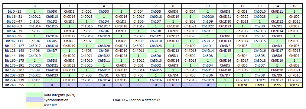
The ADAT lightpipe consists of an unidirectional optical connection, carrying up to 8 channels of 24 bit audio data, plus a number of auxilary data streams. The connection is divided into packets, each containing 256 bits. These packets are sent every sample point, so for an 48KHz sample rate, 48000 times a second meaning once every 20.83 microseconds. The bit rate implied by this is 12,288,000 bits per second or 12.288Mbps. This datastream is NRZI encoded for a 6.144Mbps symbol rate.
The physical interface for sending an ADAT lightpipe tream is the Toshiba TOSlink connector. This LED based connection, along with a PTFE based carrier link, can transmit ADAT up to a distance of about 10 meters and is the same that is used in an optical SP/DIF connection. However, the ADAT protocol is not backwards compatible with SP/DIF, they only share the same physical interface type.
3. Decoding ADAT
Because the data rate of 12.288Mbps is too fast for the popular TOTX173 fiber tramsit module, data is NRZI encoded by sending a '1' as a change in signal level, a '0' being sent as no change in the signal. For ensuring enough signal transitions are made, a '1' bit is sent after every 4 databits for correct decoding of the ADAT stream. This is true for almost everything about the ADAT protocol, except the synchronisation sequence. The synchronication consists of 10 '0' bits being sent, meaning a longer time that the stream stays at a defined level (being high or low level does not make a diffrence with NRZI) then anywhere else in the data signal.
With a 24 bit audio sample, this can be transmitted with this encoding scheme in 6 times a nibble-wide data chunk, each followed by a '1' bit to ensure data integrity. In all, 30 bits are used for an audio sample, and 8 of these audio samples, 240 bits out of our 256 bits are explained. Of the remaining 16, ten of those are in the synchonisation sequence, leaving 6 bits. 4 user bits can be transmitted, containing auxilary data, and this user data is encapsulated in '1' bith before and after, again for data integrity. All of the bits in the ADAT protocol are now assigned. 
4. FPGA implementation
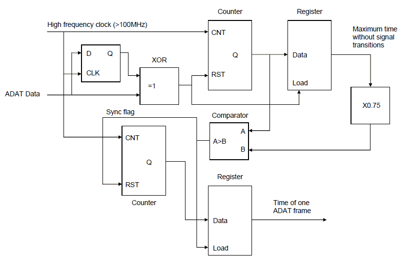
The choice is made to make the implementation of a ADAT decoder as a feed-forward receiver. This means that, apart from the data signal itself and a high frequency unrelated clock signal, the core produces its own synchronisation and support signals for correctly decoding the stream. As a start, a frame synchronising machine is needed. The sync sequence of adat are 10 bits being '0', this means that during sync there are no transitions. This is something we can measure. Take a counter, and as long as the data signal does not change, it counts up. If the data signal changes, it resets and puts the max value is a seperate register.
Next, we need a "flag" signal that changes if there is no transition for about three quarters of the "maximum time without signal transition"-register. This means that the flag signal is active when there is a constant level for 7.5 databits or up. This is only going to happen at the sync signal, because all other times the ADAT signal is going to change after 5 bits tops. Three quarters is chosen because it is binary easy to create. Take the register, bit-shift to the left and you have only half the value left. Bit-shift to the left again, and you'll have a quarter of the original value. Add one half to one quarter, and you'll end up with three quarters.
If you feed the three-quarters-signal and compare it to the transition counter, which we feed into a second counter, you will count the time it takes for the ADAT signal between two synchronisation sequences. This is a very useful signal, as it also represents the time of one complete frame. This signal we want to put in a register, a "frame time register". This completes the frame synchronication machine.
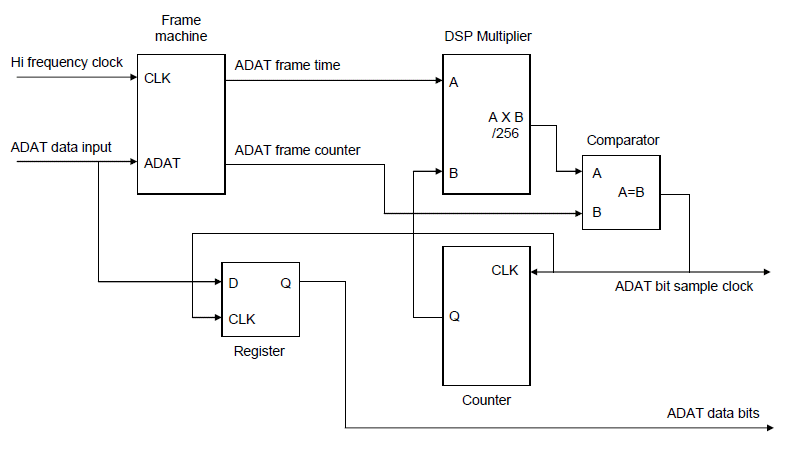
The ADAT frame time signal is at the very base of the decoding process of the ADAT signal. Next, we want to extract 256 bits out of the ADAT datastream. This can be achieved by using one of the FPGA built-in multiplier DSP blocks. If you feed the frame time register signal of 'n' bits to a multiplier, and at the other input the binary value of 1, you'll get 1/256 of the input. When you compare this value to the frame time counter value, you can count up from there on to get to the second bit, then the third, etc. To sample the ADAT input signal at the set bit times, you will get an ADAT bitstream.
In the logic analyser the bit extraction process can be made clearly visible. The bit clock moment is a small pulse, at which the data signal is latched in. The bit counter output from the DSP block is also visible.


